Aerosol Jet Printing Characteristics
Optomec’s Aerosol Jet process is an additive process, which deposits a wide variety of materials onto a wide variety of substrates without conventional masks or thin-film equipment.
Functioning is briefly reported here.
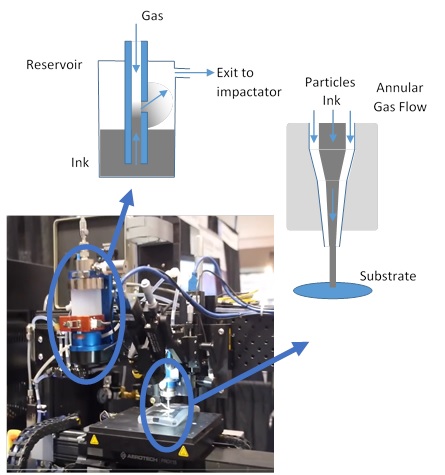
The aerosol is generated by using an ultrasonic transducer or a pneumatic nebulizer. For the generation of aerosols from low viscosity suspensions, the ultrasound transducer is usually preferred. The main reason is the fact that much less of 1 ml of suspension is required for processing. For high viscosity suspensions up to 1000 cP (comparable to the viscosity of honey), the pneumatic nebulizer is used. After the generation, the aerosol flow is focused by means of a deposition head so as to form a coaxial flow between the aerosol stream and a gas stream which acts as a sheath. For the gas used as a sheath is employed nitrogen, because it is a relatively inexpensive inert gas, or compressed air. Because of the coaxial flow, the gas stream prevents contact of the aerosol stream with the nozzle inner layer and this avoids the clogging. In the print head, the aerosol stream, which consists of many individual droplets, is concentrated up to a tenth of the nozzle diameter. Using a nozzle diameter of 100 microns, a width of lines of less than 10 microns may be generated. The aerosol can be deposited on the planar surfaces and on surfaces not planar moving the print module relatively to the substrate surface. After the deposition, the structure can be sintered laser.
Characteristics
- Line widths from 10 μm to 100s of μm per pass.
- Single pass layer thickness of 100 nm – 10 μ
- Material “ink” operating viscosity range from 1 – 1000 cP, offers the widest range of material selection on the market.
- Aerosol Jet technology utilizes an annual sheath gas to direct the droplets to the substrate. Since the droplets do not touch the nozzle, there is much less propensity for material to clog in the nozzle.
- Droplet diameter sizes from 1-5 μm offers uniform printing dispersion.
- Ability to print materials with conductive material loading up to 70 wt%. This is a key advantage over other electronic printing technologies since it offers higher conductivity in one pass.
- Print nozzle standoff to substrate distance of up to 5 mm allows printing over surface irregularities and contours. Maintaining constant feature width over a 5 mm distance enables access to corners.
Aerosol Jet Printing Vs. Inkjet
Different aspects can be found between the two technologies.
| Aerosol Jet | Inkjet |
| Clog resistant nozzle | Clogging nozzle |
| High density micro droplets = 1-5 microns | Low density inks |
| Continuous stream | Single large drop = 30 micron |
| Tightly focus | Random directions |
| Wide viscosity range = 1 to 1000 cP | Reduced viscosity range = 8 to 12 cP |
Inks
Aerosol Jet is also capable of depositing a variety of materials as dielectrics, epoxies, polymers, conducting materials, carbon nanotubes, etchants, and adhesives; as well as the ability to print biological material.
| Metal Conductors | Ceramics & Oxides |
| Nano Ag, Nano Au, Nano Pd, Thick Flim Au, Cu & Al | Yttria Stabilised Zirconia, Barium Titanate Particulate material Ceramic precursors (BaTiO3), Al2O3, RuO2, TiO2, SiO2, InSnO2, other metal oxides, … |
| Metal Alloy/Composite Material | Nano-Particles Composites |
| Ag Conductive Adhesive CuNiMn | TiO2 in PLGA (Polylactide-co-glycolide), TiO2 in SolGel, SolGel + nano-TiO2+ZnS, PTF with Barium Titanate |
| Conductive Polymer | Dielectrics |
| PEDOT:PSS, Carbon Nanotubes (CNT) | UV Epoxy, PMMA (Polymethylmethacrylate), PVP (Polyvinylpyrrolidone), Polyimide, PTFE |
| Organic Semiconductor | Biomaterials |
| P3HT (in organic photovoltaics), PQT (in thin film transistors), CNT, … | Peptides &Proteins, Antibodies, DNA, Prokaryotic cell, E.coli, Simple eukaryotic cell (yeast), Mammalian cells (3T3, HDF) |
| Resistor | Novel Materials |
| PTF (Polymer Thick Film) Carbon, Metal Oxides | Etch materials & Etch resists, Solder Mask, Photopolymerizable SolGel |
Photonic Curing
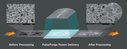
An essential aspect concerning the design and construction of devices with printed electronics is the curing and sintering system. The market leader for this sector is Novacentrix AUSTIN TEXAS (USA), which sells photonic sintering machines. This new and unique technology makes it possible to create innovative electronic devices on substrates that up until now could not be used due to incompatibilities with classic manufacturing processes.
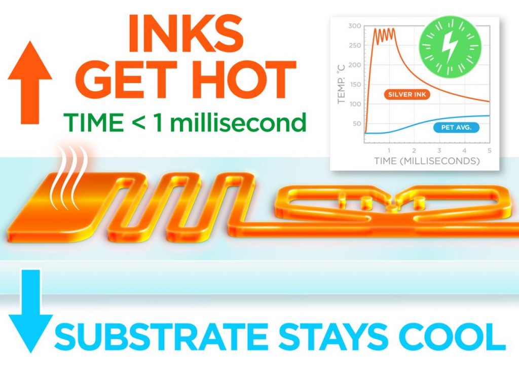
This technology is able to sinter a thin film by heating it with pulsed light through a flash lamp. When the film is heated on a substrate, most of the substrate remains relatively cold because the exposure time is short (~ 1 ms). When this transient processing is performed on substrates with low flame temperatures, such as plastic or paper, it is possible to reach significantly higher temperatures in the thin film without damaging the substrate than is possible with a normal oven. Because light-curing instruments rapidly polymerize thin films at high temperature on low-temperature substrates, it is ideal for reel-to-roll processes on polymer or paper.
The light-curing was developed for the first time by NovaCentrix and is incorporated into the PulseForge® tool set. It has become a fundamental manufacturing process in the production of printed electronics as it allows for economical and flexible substrates that cannot be used with classic sintering technologies. Furthermore, the higher processing of the temperature offered by the light-curing reduces the processing time exponentially, often from minutes to milliseconds, which increases the whole productivity while maintaining a very small footprint of the machine.